Light-induced quantum condensates on a chipHow can we turn light (photons) into artificial quantum matter (Bose-Einstein condensates or quantum liquids) inside semiconductor nano-structures? |
||

|
Excitonic quantum fluid devices:Boson-like quasi-particles (excitons) in semiconductors are well known for many years, however it is still an open question how exactly would such quasi-particles behave in the limit where quantum statistics takes over. Can new states of matter be found in such systems? If so, how would their sometimes intricate structure, different dimensionality, and very different physical properties, as well as the various and complex interactions inside their host material, affect their nature, and what kind of new (and hopefully also unexpected) emerging phenomena would be displayed as a result?Our main goal is the fundamental study of manipulation and control of two-dimensional exciton quantum fluids, in the Bose degeneracy limit, in various new electro-optic flow devices. Developing a set of tools for manipulating, controlling, trapping, and transporting dipolar excitons over large distances and long times, is crucial to achieve a sufficient level of control to create conditions necessary for the understanding of the macroscopically condensed state, as well as to explore the possibilities of future excitonic devices and circuits for photonics applications, based on macroscopic quantum coherence. |
|

|
Key directions: |
|

|
Vision:We hope that our research will help to both better clarify the nature and properties of the emergent macroscopically coherent state of excitons and its effect on the exciton dynamics and on the electro-optic device properties, and that it would lead to new, proof-of-concept exciton electro-optic devices for future applications based on the new methodology of exciton quantum fluids. |
|
|
||
Harvesting quantum lightHow light and nano-matter interact on the quantum level, and can we use it for making ultrafast single photon sources and nano-optical devices for quantum information? |
||

|
Active single photon devices:Our interest in this research effort is to understand the unique locally enhanced electromagnetic behavior of electronic and photonic modes in nano-patterned metallic and dielectric structures and show how they can be coupled in a controlled fashion to nano- emitters. These nano-emitters have a well-defined quantum mechanical electronic structure which must be effectively integrated with the nanostructures of interest. Our studies of these effects have been implemented to design and demonstrate novel devices that will have a potential impact on various application fields. One such device is a structure combining a strong plasmonic enhancer (plasmonic nanocone resonator) and a highly directional nanoantenna (bullseye). This device is deterministically coupled to single nano emitters to produce a high-rate stream of single photons. Another application could be to use tiny elements, based on active photonic, plasmonic, or hybrid plasmonic-photonic devices, that could be externally controlled. Near field techniques can also be used to optically, electrically, or magnetically target specific areas on functionalized photonic or plasmonic devices, with nanometric resolution, allowing in-situ control of the device functions. |
|

|
Key directions: |
|

|
Vision:We are trying to build novel quantum optical devices by coupling quantum emitters to various photonic and plasmonic resonators. This will hopefully have many quantum applications in the fields of quantum cryptography and metrology. |
|
|
||
Mixing light and matter for future quantum opto-electronicsHow to make new quasi-particles which are half-light half-matter? |
||

|
Exciton polaritons:Fascinating quantum quasi-particles that emerge when electronic excitations inside semiconductors (named excitons) strongly interact with photons. These part-light part-matter quasi-particles have some very interesting physical properties: While their photonic part yields a very small effective mass, a large thermal De-broglie wavelength, and very large group velocities, Their excitonic part allows them to interact with external fields (such as electric and magnetic fields) as well as with each other, via particle (exciton-exciton) interactions. These properties made exciton polaritons a compelling system for studying many fundamental quantum-collective phenomena at elevated temperatures, leading to the observation of polariton Bose-Einstein condensation, polariton-solitons, and polariton lasing among others. In addition, these properties are also promising for realization of new polariton based logic circuitry which, if successful, would enable extremely fast transfer and processing of coherent information packets. In our lab we engineer “flying” polariton systems where polaritons are confined in dielectric waveguides and are polarized by external fields to form dipolar exciton polaritons (“dipolaritons”). This allows us to study the behavior of dipolaritons as single particles and their mutual interactions at the high densities. Such waveguide dipolaritons can be controlled and manipulated both through their excitonic part and their photonic part, and show promise for the implementation of feasible polaritonic devices. |
|

|
Key directions: |
|

|
Vision:We hope to understand how these electrically controlled waveguided polaritons can be utilized as a platform for both for the fundamental study of various many-body quantum phenomena, and for the implementation of future polaritonic based logic circuitry. |
|
|
||
Applied opticsNew concepts in optical probing of material properties and thin film thicknesses with high lateral resolution for industrial and scientific applications. |
||

|
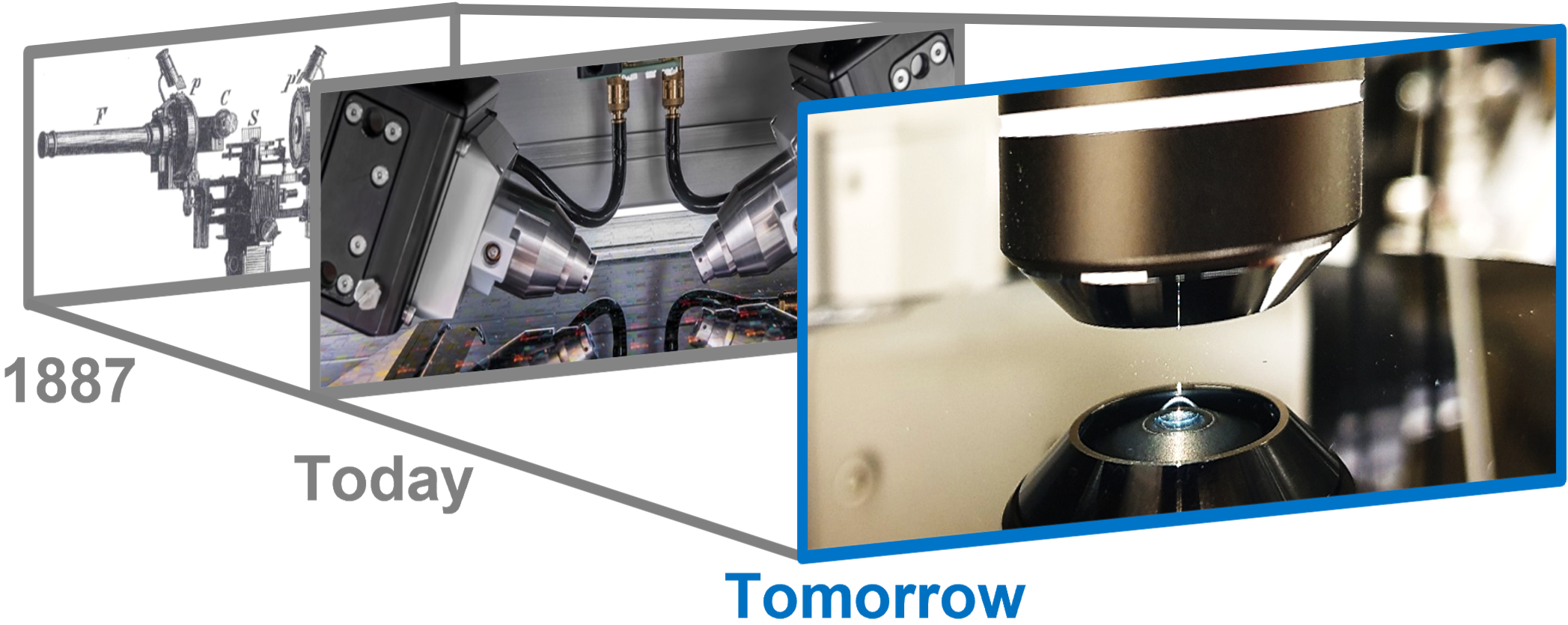
Spectroscopic Micro-Ellipsometry:Ellipsometry is a measurement technique for determining optical constants and thickness of various optical materials and thin films with an extremely high accuracy down to atomically thin layers. Today, standard ellipsometry methods have low lateral resolution or very slow data acquisition, thus they cannot easily detect and measure small, micron-scale surfaces. This is a major limiting factor of this technology.We are developing a new concept and technique for ellipsometry-based micro-measurement, which allows to accurately and quickly obtain local optical and physical properties with a few microns lateral resolution, so we can accurately map micron-scale surfaces and devices. Our instrument can also be used to determine the number of layers of two-dimensional materials such as graphene, down to a single layer of atoms or molecules. |
|

|
Key directions: |
|

|
Vision:High speed, scanning, spectroscopic micro-ellipsometry with high lateral and temporal resolution aims to play a major role in material characterization both in science and technology. We aim for a compact device capable of accurate and fast determination of material properties with high lateral and temporal resolution. This will open the way for exciting applications such as measuring time-dependent thickness changes for newly developed ultra-thin materials, characterizing single atomic layer materials (such as graphene, hBN and TMDs) currently being studied by many research groups and considered to play a major part in future technologies, detecting defects on semiconductor wafers with very high speeds to boost the production rate and quality in semiconductor industries. |
|
Light-matter interaction in flatlandHow can we use combinations of two dimensional layered materials to create tiny devices with new engineered properties? 
|
||

|
Multi-layer semiconductor heterostructures:Van der Waals materials, also known as layered materials, are built of layers of atoms with strong covalent in-plane bonds, and weak coupling forces in between individual layers. These weak interlayer forces make it relatively easy to isolate a single atomic layer (a.k.a. monolayer) of these materials. Stacking monolayers of two (or more) different materials one on top of the other can result in optical and electronic properties that are absent in the individual layers which form the structure. By carefully choosing the materials and the order of layers we can create, using light, a special kind of matter excitations called two-dimensional excitons (which are bound pairs of energetic electrons and the vacancies they leave at lower energies, which are named holes). A special type of excitons appear only at the interface of two layers. They are known as interlayer excitons. A characteristic feature of such excitons is a permanent dipole-moment, which opens the gate to study new many body dipole-dipole interactions. |
|

|
Key directions: |
|

|
Vision:We hope to better understand the nature of the different excitons in our multi-layer heterostructures. Understanding the properties of these excitons may lead towards observation of Bose-Einstein condensates as well as opto-electronic devices with new functionalities. |
|
Recent work from our group
|
||
| Thickness mapping of exfoliated vdW materials by micro-ellipsometry | ||
| Guided Dipolar Exciton-Polaritons | ||
| High Brightness Single Photon Sources | ||
| Purification of single photons by temporal heralding of quantum dot sources | ||
| Attractive dipolar coupling between stacked exciton fluids.pdf | ||
| Dynamic formation of a strongly correlated dark condensate of dipolar excitons | ||
| Room-temperature ultrabright single photon sources for free space and fiberbased applications | ||
Popular Views
|
||
|
June, 2023: Our work recently published in ACS Nano was under the spotlight by several popular science and news websites, including PHYS.org,
EurekAlert!, AZoNano,
Nano Werk, ScienMag,
Bioengineer.org and Mirage News. |
||
|
March, 2023: Our recently published paper in Review of Scientific Instruments was covered by the popular Israeli science website Hayadan.org.il (in Hebrew). |
||
|
February, 2023: Our paper "Mapping spectroscopic micro-ellipsometry with sub-5 microns lateral resolution and simultaneous broadband acquisition at multiple angles" was selected as a featured paper for special highlight on AIP Scilight. |
||
|
November, 2021: Our work recently published in ACS Nano was under the spotlight by several science and news media outlets, including PHYS.org,
EurekAlert!, AlphaGalileo,
Florida News Times, The Jerusalem Post
and Israel Hayom (Hebrew). |
||
|
November, 2021: Our work on exciton superfluids and supersolids was covered by the popular website of Israel Science Foundation (in Hebrew). |
||
Collaborators |
||


